
Key ideas and motivation
First proposed in 2005, scalable planar Penning traps were originally developed with quantum computing in mind, using trapped electrons as qubits. Our vision is much broader. Scalable and portable Penning trap technology could open up new opportunities in quantum sensing, high-precision mass spectrometry, microwave spectroscopy and fundamental physics.
Conventional 3D Penning traps have already shown what this technology can do. However, they usually depend on experimental set-ups that are very large, heavy and costly, often around one cubic metre, over a tonne in weight and beyond the reach of most laboratories or small and mid-size companies.
Our mission is to make Penning traps more deployable, less complex and more affordable, so that a much broader range of users in industry and academia can use them in a wider range of settings. Planar Penning traps will also open many new applications, such as quantum radar, inviable with current conventional Penning traps.
The challenge: from a 3D technology to a 2D scalable ion trap
Penning traps are built around two key elements: a magnetic field source and a set of electrodes held at DC voltages. Together, they create the forces needed to confine charged particles, including electrons, protons and ions.
Our first key idea is to translate the electrodes of a conventional trap into a flat, chip-based design. This preserves the axial symmetry of the conventional trap, as illustrated below.
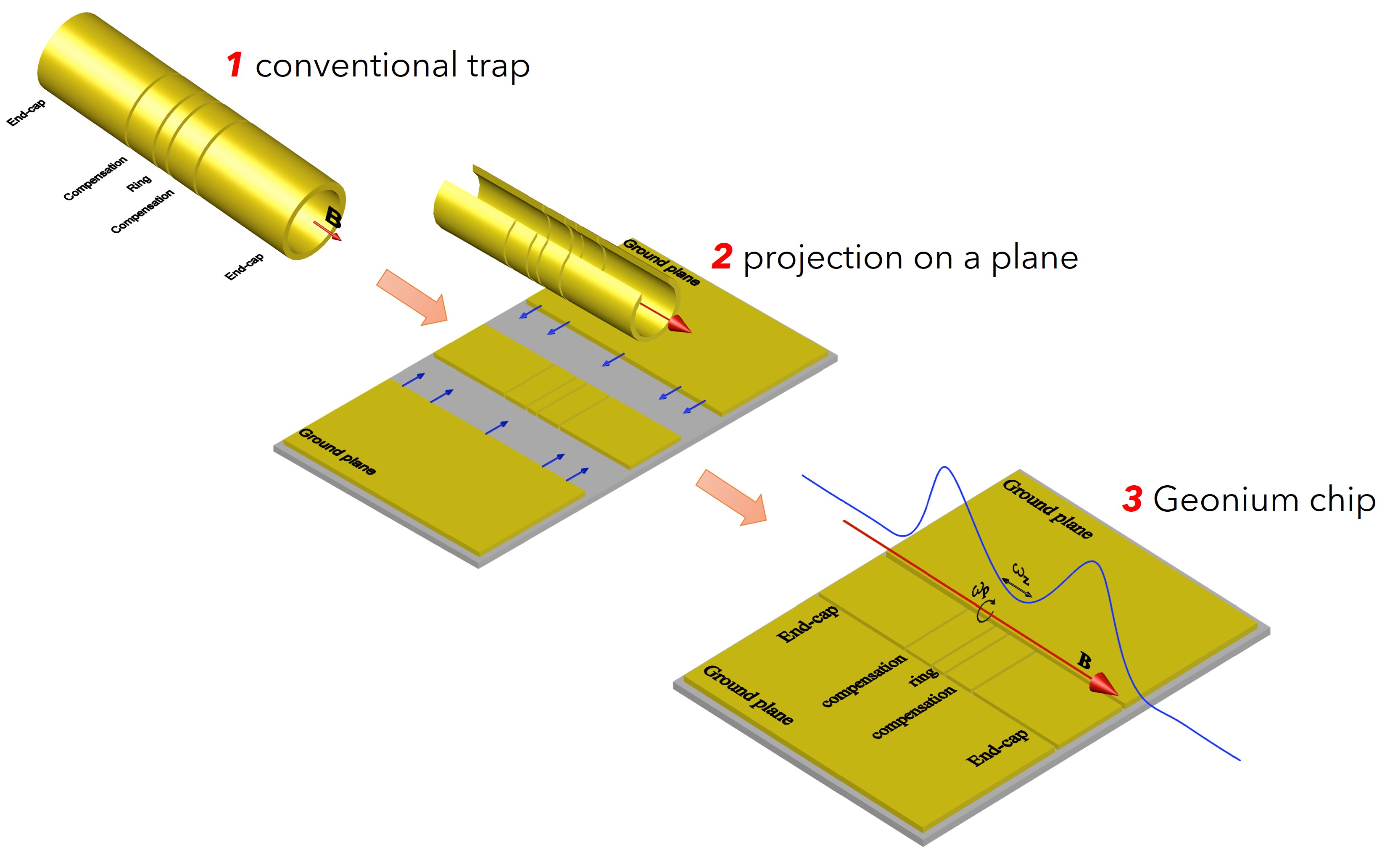
The result is the geonium chip planar Penning trap. Why this symmetry-preserving transformation matters is explained in detail in our seminal paper Theory of the Coplanar-Waveguide Penning Trap.
Geonium chip with integrated particle detection electronics
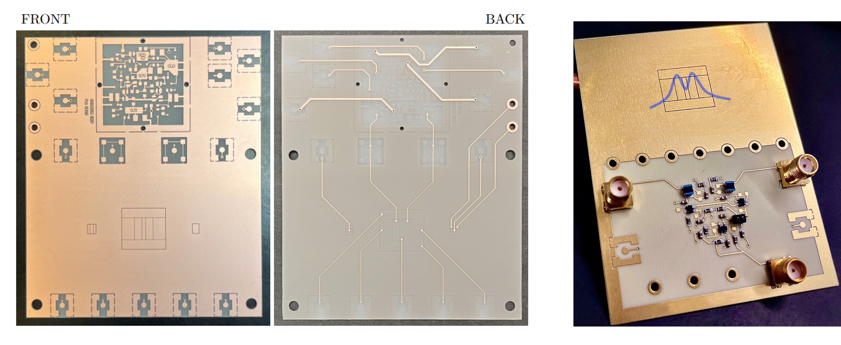
The geonium chip can be fabricated using conventional PCB technology. Careful material selection is essential for detecting the trapped particles, which is achieved with an ultra-low-noise cryogenic amplifier integrated into the chip. Details about the RF properties of the chip is given in our article High frequency properties of a planar ion trap fabricated on a chip.
Compact cryogenic vacuum chamber
We have designed the geonium chip to act as the flange of the vacuum chamber where the particles are trapped. The chamber is evacuated through a pinch-off tube connected to a pump. Once the required vacuum is reached, it is assembled with the superconducting magnetic field source.
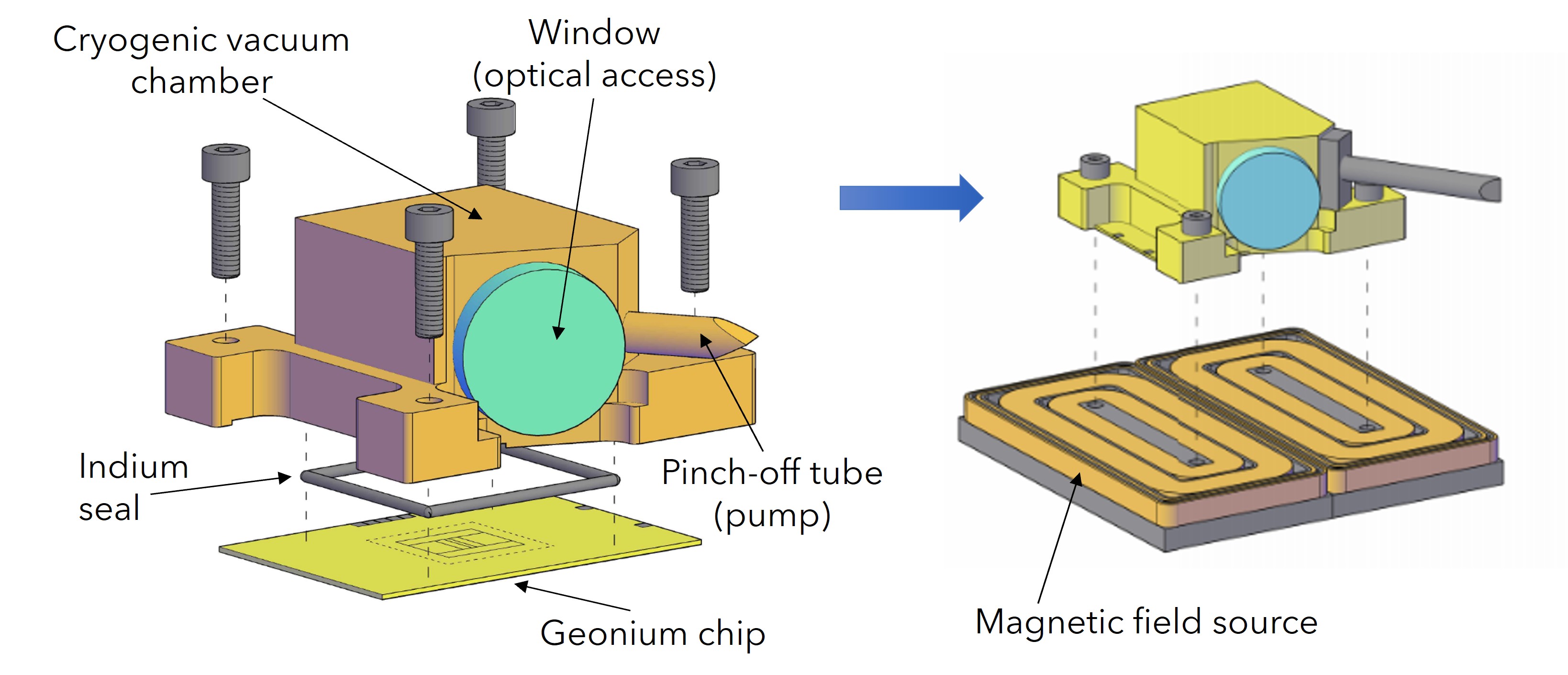 This rig is then installed in a cryostat, and ready to operate.