
The Geonium Chip project is organised into several tightly connected research areas, each addressing a critical component of the broader mission: to make Penning trap quantum technology compact, affordable, and scalable.
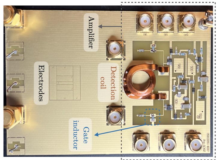
Scalable chip Penning traps
We develop and operate planar Penning traps fabricated on a chip integrated with RF/MW electronics to enable precise control and detection of single electrons (or other charged particles) at cryogenic temperatures. Our chips are also designed to act as the flange for the small cryogenic vacuum vessel surrounding the particle trapping region.
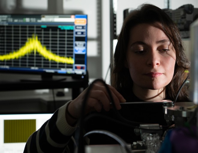
Quantum microwave sensors with trapped electrons
We pioneer the use of a trapped electron as a quantum sensor and emitter of microwave photons. This system offers single-photon sensitivity across a broad range of GHz frequencies, along with tunability, generation of multiphoton quantum states, and other key advantages. The applications are very broad. We are investigating the implementation of a quantum radar.
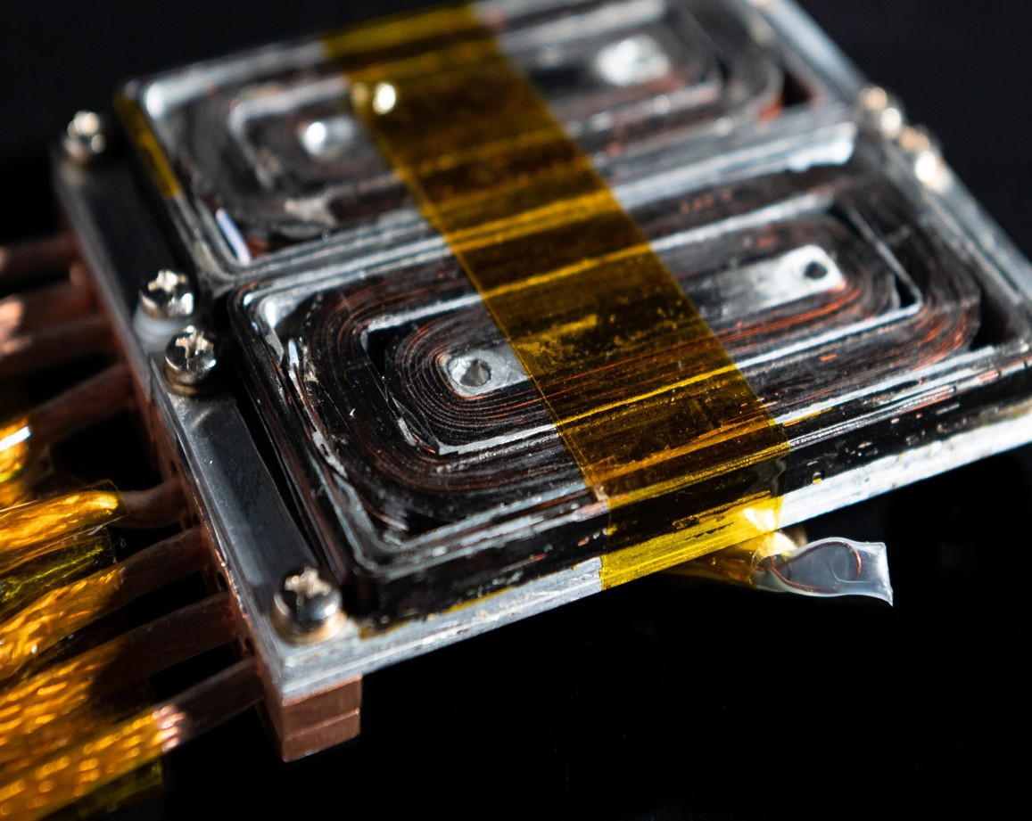
Planar superconducting magnetic field sources
Our vision is that Penning trap technology can only become truly scalable if the magnetic field source is scalable too. By replacing the large superconducting solenoids used in conventional traps, we can make Penning trap systems smaller, more practical and easier to deploy. Our novel planar magnets also have potential applications well beyond ion traps.
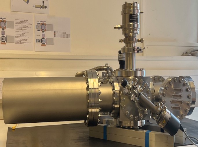
Portable cryogenic platforms
Thanks to our pioneering planar magnetic field source, the Geonium Chip can operate with compact Stirling cryocoolers, eliminating the need for bulky liquid helium cryostats. This will dramatically reduce system complexity and footprint, making the Geonium Chip a viable platform not just for research labs, but also for mobile and field-deployable quantum technologies.